How to Optimize Your Pcb Printed Circuit Board Design for Maximum Performance
In the rapidly evolving landscape of electronics, optimizing your
PCB Printed Circuit Board design for maximum performance is not just an option
but a necessity. According to a report by MarketsandMarkets, the global PCB market is projected to grow from
$60.3 billion in 2020 to $76.5 billion by 2025, driven by
advancements in technology and increasing demand for electronic devices. As the complexity of circuit designs increases,
the need for efficient layouts, enhanced thermal management, and impedance control becomes critical. A well-designed PCB
can significantly impact the reliability and longevity of electronic products, reducing signal loss and manufacturing costs.
This blog will delve into essential strategies and best practices to ensure that your PCB Printed Circuit Board meets the
performance benchmarks required in today's competitive market.
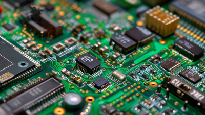
Understanding the Basics of PCB Design for Enhanced Performance
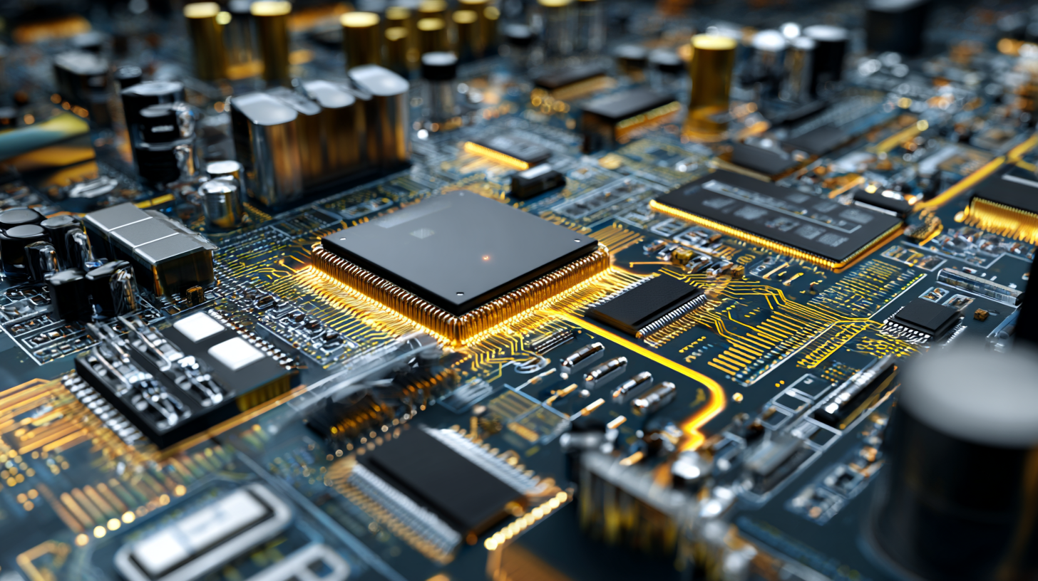
When diving into PCB design, understanding the foundational concepts is crucial for enhancing performance. A well-structured design not only ensures functionality but also contributes significantly to reliability and efficiency. One of the primary considerations is the layout. Keeping traces short and direct minimizes inductance and capacitance, which can lead to faster signal transmission and reduced noise.
Tip 1: Use proper trace widths according to the current they will carry. This aids in preventing overheating and ensures that your design can handle the required electrical load. It’s essential to refer to trace width calculators to maintain optimal dimensions based on your specific needs.
Another vital aspect is component placement. Strategically positioning components can reduce interference and improve heat dissipation. Arrange high-frequency components centrally, while providing adequate spacing between sensitive analog circuits and noisy digital ones.
Tip 2: Incorporate thermal relief pads for components that generate heat. This practice helps distribute heat more effectively, protecting sensitive areas of the PCB from thermal stress.
By focusing on these fundamental principles of PCB design, you can drive your project toward maximum performance and longevity.
Key Factors Influencing PCB Layout and Optimization Techniques
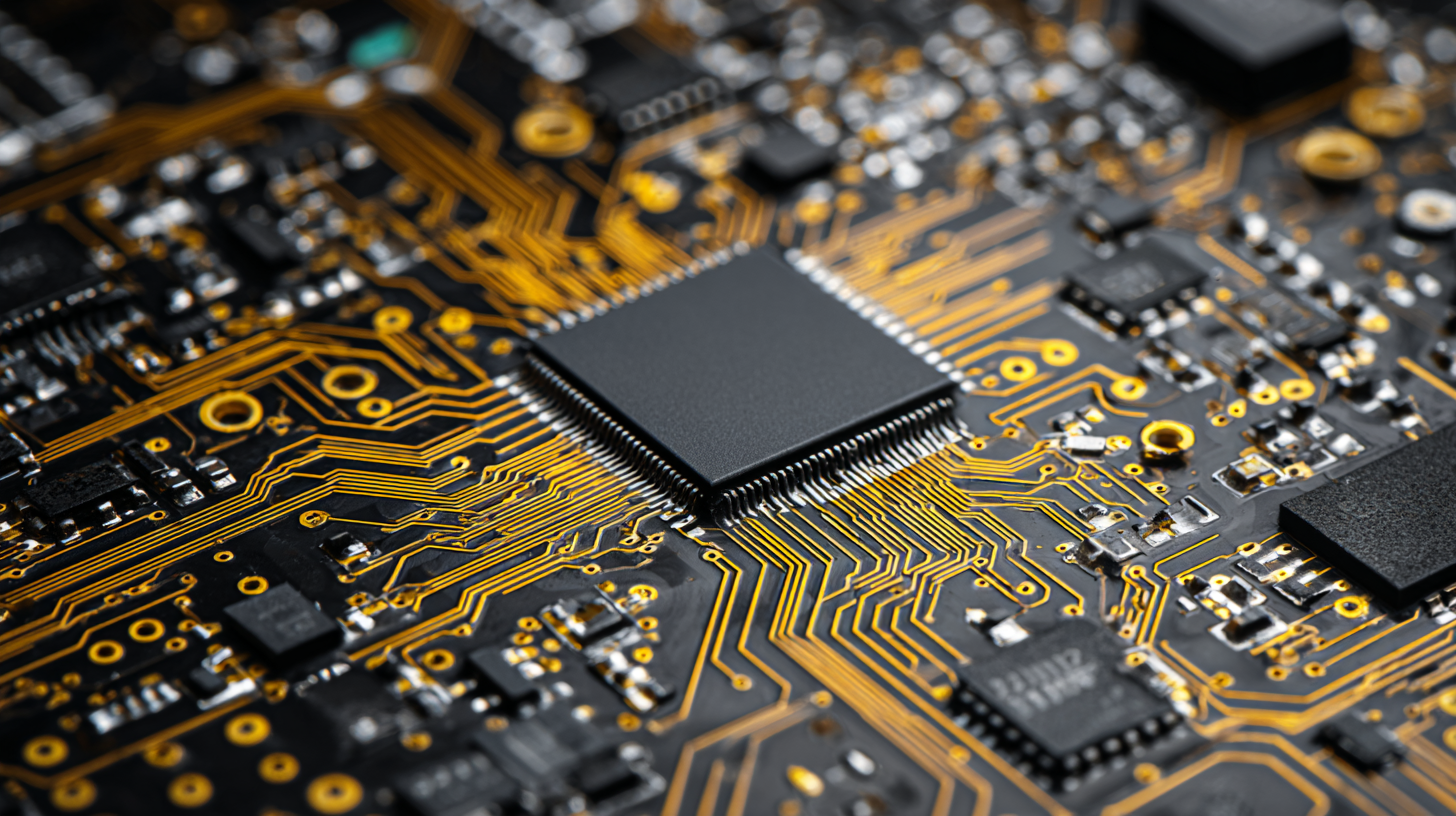
When optimizing PCB layouts for maximum performance, several key factors come into play that are fundamental to achieving high efficiency and functionality. One primary consideration is the arrangement of components, which significantly influences signal integrity (SI) and power integrity (PI). By strategically placing components to minimize signal path lengths and using ground planes effectively, designers can enhance performance. Moreover, maintaining appropriate trace widths and spacing is crucial to reduce resistive losses and achieve better thermal management.
Another vital aspect of PCB optimization is the management of electromagnetic interference (EMI). Effective shielding and thoughtful routing can mitigate EMI effects, ensuring that signals remain clean and unaffected by noise. The rise of advanced simulation techniques, especially in the context of AI-driven design tools, has enabled engineers to better predict performance outcomes before physical prototypes are built. As industries adopt these technologies, the integration of multi-physics simulations in the design process is becoming increasingly necessary to address the complex challenges posed by modern electronic products, particularly in the realm of 5G applications and high-speed circuits.
Advanced Materials and Their Impact on Circuit Board Performance
When designing PCB printed circuit boards, the choice of materials plays a crucial role in determining performance. Advanced materials, such as high-frequency laminates and:
- **Tip 1: Consider Dielectric Properties** - Selecting materials with low dielectric constants can significantly reduce signal loss and improve the overall speed of the circuit. This is particularly important for high-frequency applications, where even minor losses can lead to major performance issues.
Another important consideration is the thermal management of the PCB. Materials with superior thermal conductivity ensure that heat generated by the components can dissipate effectively, maintaining optimal operating conditions.
- **Tip 2: Utilize Thermally Conductive Substrates** - Using substrates that conduct heat well will help safeguard sensitive components. Synthetic materials like aluminum or copper-clad laminates can enhance heat dissipation and extend the longevity of the circuit board.
Ultimately, the integration of advanced materials can elevate your PCB design's performance by addressing issues like signal integrity and thermal management. Embracing these advancements not only optimizes the performance but also paves the way for compact and efficient circuit designs.
How to Optimize Your Pcb Printed Circuit Board Design for Maximum Performance
| Material Type |
Layer Count |
Thermal Conductivity (W/m·K) |
Dielectric Constant |
Mechanical Strength (MPa) |
Cost per Square Meter (USD) |
| FR-4 |
4 |
0.25 |
4.2 |
400 |
20 |
| Rogers 4350 |
6 |
0.45 |
3.5 |
550 |
45 |
| Polyimide |
2 |
0.30 |
3.0 |
700 |
60 |
| PTFE |
8 |
0.20 |
2.1 |
500 |
80 |
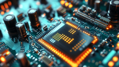
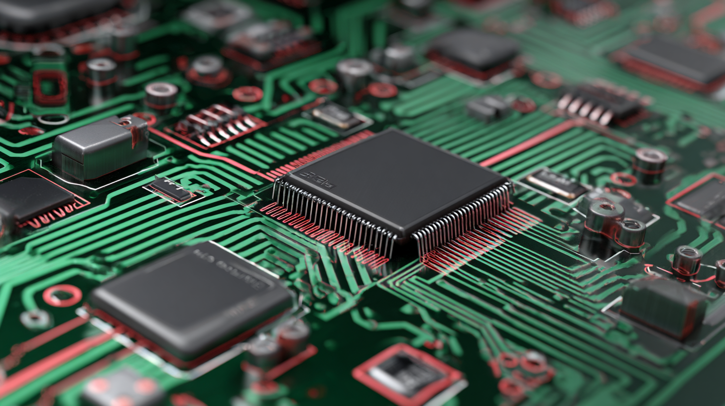
Best Practices for Routing and Component Placement in PCB Design
When it comes to optimizing your PCB design for maximum performance, effective routing and component placement are crucial. Thoughtful arrangement can significantly minimize electromagnetic interference (EMI) and signal degradation. Start by placing sensitive components away from high-frequency traces to reduce noise. Additionally, ensure that your power and ground planes are as solid as possible to create a stable reference for all components.
**Tip:** Keep traces short and direct to pass signals efficiently. Avoid 90-degree angles in your traces, as they can lead to signal reflection. Instead, use rounded corners to create smoother transitions.
Another critical aspect is managing thermal dissipation. Position heat-sensitive components away from heat-generating parts, allowing for better airflow and heat management. Routing also plays a role in thermal performance; use wider traces to dissipate heat more effectively and prevent potential hotspots.
**Tip:** Implement vias wisely, allowing for effective heat transfer between layers. When routing multilayer PCBs, consider using buried or blind vias to maintain signal integrity and avoid clutter. By following these best practices, you can enhance the performance and longevity of your PCB designs.
Testing and Iterating Your PCB Design for Optimal Functionality
When it comes to achieving optimal functionality in your printed circuit board (PCB) design, testing and iteration play crucial roles. The initial design phase is just the starting point; rigorous testing is essential to identify weaknesses or potential failures. Utilizing techniques such as simulation software can help predict how your circuit will behave under various conditions, allowing you to make informed adjustments before moving forward. Additionally, creating prototypes is a vital step that can reveal unforeseen issues, enabling you to observe real-world performance and functionality firsthand.
Iteration is key in refining your design. After testing your initial PCB prototype, gather data on its performance and identify areas for improvement. Consider conducting stress tests to assess how the board handles thermal and electrical loads. Feedback from these trials can inform design changes, such as layout adjustments or component selections. Engaging in this cyclical process of testing and iterating not only enhances the reliability of your PCB but also maximizes its performance, ensuring that it meets both design specifications and user expectations.